
Technology
SiC
The use of silicon carbide (SiC) in electric vehicles (EVs) is certainly in the spotlight right now. The combination of unique SiC material properties enables engineers to develop components that are smaller, more efficient, and more reliable compared to silicon counterparts. This enables increased power density, reduced power loss, increased driving range, and at the same time a reduced weight and cost of the electric vehicle. Most of the car manufacturers have already announced that within a decade they will phase out the development of internal combustion engines and will go all-electric. Such news led to huge investments in the development of SiC crystal growth and device fabrication technologies. However, despite all the efforts, the demand for this material is still growing faster than the supply.

SiC properties
SiC has 10 times higher breakdown electric field strength (Emax) as compared to that of Si. The higher the Emax, the thinner the drift layer, and the higher the doping. A unipolar device of SiC has, theoretically, 1000 times lower on-resistance than its Si counterpart.

Most common SiC crystal growth techniques
PVT – Physical Vapor Transport
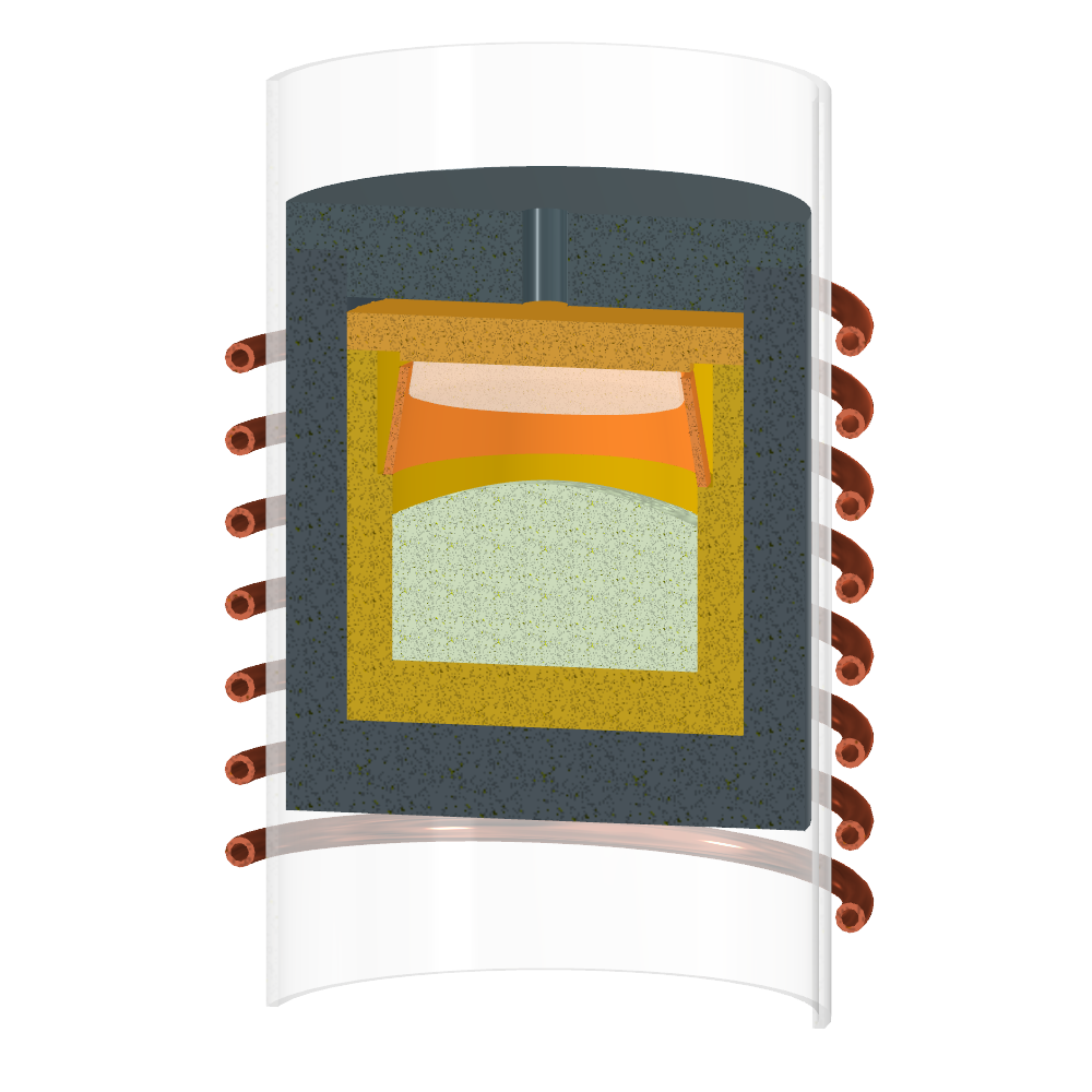
PVT is the most common silicon carbide (SiC) bulk crystal growth technique. The crystal is grown in a graphite crucible that is loaded with SiC source material at the bottom and a SiC seed crystal at the top. As the temperature increases beyond 1800 °C, the SiC source material starts to sublime appreciably. The sublimed specie are transported towards the slightly colder seed, where they condense to form a SiC crystal.
Simple yet hard to master.
The technique may seem simple, yet it is essential to have full control of the process pressure, temperature, thermal gradients, seed quality, and the source material, in order to obtain a high-quality crystal.

CVD – Chemical Vapor Deposition
The SiC crystals are sliced and polished into substrates and then they are ready for epitaxial growth of high quality films with highly controlled doping and thickness.
Chlorinated chemistry enables high growth rates.
Formerly, CVD of SiC used precursor gases such as silane and propane diluted in a massive flow of hydrogen, however in the pursuit of higher growth rates, the chemistry changed to include chlorinated precursors to avoid homogeneous nucleation, i.e. particles in the gas phase. The chlorinated chemistry enables an increase of the growth rate from about 10 µm/h to 100 µm/h. The most commonly used precursors are today trichlorosilane and propane or ethylene.
HTCVD – High Temperature Chemical Vapor Deposition
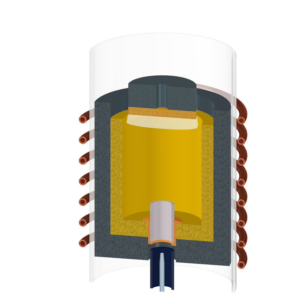
The HTCVD technique is, just like the PVT technique, a sublimation technique, but the source material is introduced as reactive gases in an injector at the bottom of the hot zone. The carrier gas flow is very small and hence the concentration of the precursor gases is high. Homogeneous nucleation is therefore pronounced, and the precursor gases react already in the injector to form micro-particles of SixCy in the gas flow. The micro-particles are moved by the carrier gas to the hottest part of the crucible, where they sublime and subsequently get transported to the colder substrate, where they condense.
Ultimate control and high purity.
The main advantage of this technique is the high purity of the material, the control of the C/Si ratio, which helps to improve the crystal quality, and the possibility to observe the growth through the viewport installed below the injector.